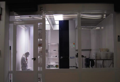
This facility has been designed for measuring stress and failure evolution in thin films and thin film structures deposited on wafer substrates. Problems involving the processing and operation of thin-film structures in microelectronic and optoelectronic applications are of interest. Coherent gradient sensing (CGS) shearing interferometry is used for measuring curvature and inferring stresses in these structures. The facility is in a Class 1 cleanroom and is capable of measuring patterned wafers up to 300mm in diameter.